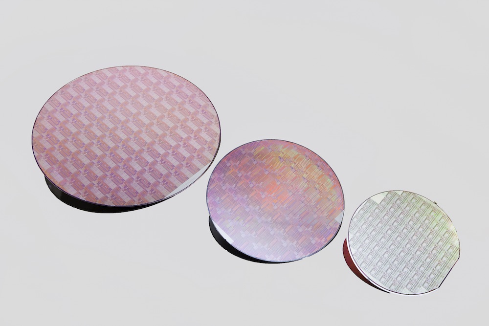
 Though Gallium Nitride (GaN) has been making headlines for the past several years as an emerging RF technology, RF semiconductors developed with silicon, namely RF silicon-on-insulator (RF-SOI), has also been advancing as a semiconductor of choice for the exploding RF hardware markets.
Where GaN is a still relatively expensive and small wafer technology, RF-SOI is largely compatible with mainstream silicon fabrication processes. Therefore, RF-SOI benefits from the high volume and well established large wafer silicon process technology development. The results of this are that RF-SOI technologies, though they don’t exhibit the extreme high power and frequency capabilities of RF GaN semiconductor devices, are increasingly prevalent in consumer and automotive wireless electronics. The expanding adoption of consumer wireless electronics, such as smartphones, Wi-Fi routers, Bluetooth chips, automotive radar, and other Internet-of-Things (IoT) RF hardware. Mainly, RF-SOI semiconductors are used as RF Front-End (RFFE) modules, switches, antenna tuners, filters, varactors/diodes, and passives (resistors, inductors, capacitors, and transmission lines).
Recent advances in RF-SOI have led to SOI technologies with enhanced signal integrity features that are suited for LTE-Advanced and 5G mid-band (~1 GHz to 7.25 GHz). There are also RF-SOI processes that are lower performing, and are better suited to cost sensitive applications, such as 2G, 3G, 2.5 GHz WiFi low throughput, and lower throughput/power IoT applications.
Adoption of System-in-Package (SiP) technology built with physically distinct blocks of silicon intellectual property (IP), or heterogeneous integration technology (HIT), is also leading to increased use of silicon in RF applications. In this way, highly integrated silicon chiplets can be combined with silicon processes that are better suited for RF applications within the same package, which both reduces cost, size, and enables more fully featured SiP solutions.
Another silicon solution that is increasingly viable for RF applications is System-on-Chip (SoC) technology, which goes a step further than SiP technology by assembling a single complex chip from multiple IP blocks. Given the complex nature and extremely tight tolerances involved, SoC technology is typically a more expensive process, but can yield high performance SoCs with a wide range of features.
The benefits of System-on-Chip (SoC) and SiP technology have even garnered the interest of Defense Advanced Research Projects Agency (DARPA), which is attempting to standardize silicon IP for use with SoC and SiP technology, the Common Heterogeneous Integration and Intellectual Property Reuse Strategies (CHIPS) program. The goal of this program is to “establish a new paradigm in IP reuse,” in response to the enormous growth of the telecommunications market and semiconductor industry moving toward enhanced integration of the domains (digital, analog, and power).
There are also two technologies that have the potential to push silicon semiconductors into the millimeter-waves. Namely, 3D through-silicon vias (TSVs) and integrated electromagnetic interference (EMI) shielding. 3D TSVs enable the interconnecting of wafer-level stacked devices in a way that is extremely small form factors and presents good electrical characteristics. With 3D TSV technology SoCs, and otherwise higher transistor integration density technologies, can be produced at lower cost than other interconnect strategies. Similarly, integrated EMI shielding can enable higher performing SoCs and SiPs whose distinct blocks are less susceptible to external interference and emit less interference that could impact nearby subsections and circuits.


 Pasternack Blog
